- 您现在的位置:买卖IC网 > Sheet目录3753 > ATMEGA169P-16MUR (Atmel)IC MCU AVR 16K 16MHZ IND 64QFN
128
8018P–AVR–08/10
ATmega169P
15.11 16-bit Timer/Counter Register Description
15.11.1
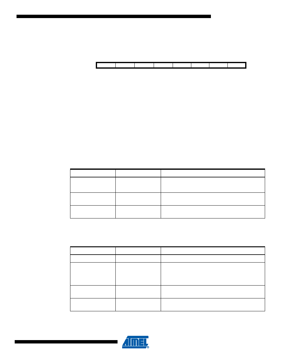
TCCR1A – Timer/Counter1 Control Register A
Bit 7:6 – COM1A1:0: Compare Output Mode for Unit A
Bit 5:4 – COM1B1:0: Compare Output Mode for Unit B
The COM1A1:0 and COM1B1:0 control the Output Compare pins (OC1A and OC1B respec-
tively) behavior. If one or both of the COM1A1:0 bits are written to one, the OC1A output
overrides the normal port functionality of the I/O pin it is connected to. If one or both of the
COM1B1:0 bit are written to one, the OC1B output overrides the normal port functionality of the
I/O pin it is connected to. However, note that the Data Direction Register (DDR) bit correspond-
ing to the OC1A or OC1B pin must be set in order to enable the output driver.
When the OC1A or OC1B is connected to the pin, the function of the COM1x1:0 bits is depen-
dent of the WGM13:0 bits setting. Table 15-1 shows the COM1x1:0 bit functionality when the
WGM13:0 bits are set to a Normal or a CTC mode (non-PWM).
Table 15-2 shows the COM1x1:0 bit functionality when the WGM13:0 bits are set to the fast
PWM mode.
Note:
1. A special case occurs when OCR1A/OCR1B equals TOP and COM1A1/COM1B1 is set. In
this case the compare match is ignored, but the set or clear is done at TOP. See ”Fast PWM
Mode” on page 120. for more details.
Bit
7
6
5
4
3
2
1
0
(0x80)
COM1A1
COM1A0
COM1B1
COM1B0
–
WGM11
WGM10
TCCR1A
Read/Write
R/W
R
R/W
Initial Value
0
Table 15-1.
Compare Output Mode, non-PWM
COM1A1/COM1B1
COM1A0/COM1B0
Description
0
Normal port operation, OC1A/OC1B disconnected.
0
1
Toggle OC1A/OC1B on Compare Match.
10
Clear OC1A/OC1B on Compare Match (Set output to
low level).
11
Set OC1A/OC1B on Compare Match (Set output to
high level).
Table 15-2.
Compare Output Mode, Fast PWM(1)
COM1A1/COM1B1
COM1A0/COM1B0
Description
0
Normal port operation, OC1A/OC1B disconnected.
01
WGM13:0 = 14 or 15: Toggle OC1A on Compare
Match, OC1B disconnected (normal port operation).
For all other WGM1 settings, normal port operation,
OC1A/OC1B disconnected.
10
Clear OC1A/OC1B on Compare Match, set
OC1A/OC1B at BOTTOM (non-inverting mode)
11
Set OC1A/OC1B on Compare Match, clear
OC1A/OC1B at BOTTOM (inverting mode)
发布紧急采购,3分钟左右您将得到回复。
相关PDF资料
ATMEGA169P-16MCHR
MCU AVR 16KB FLASH 16MHZ 64-VQFN
2-1546217-0
TERM BLK RCPT 20POS SIDE 5.08MM
1-1546217-9
TERM BLK RCPT 19POS SIDE 5.08MM
1-1546217-8
TERM BLK RCPT 18POS SIDE 5.08MM
1-1546217-7
TERM BLK RCPT 17POS SIDE 5.08MM
1-1546217-6
TERM BLK RCPT 16POS SIDE 5.08MM
1-1546217-5
TERM BLK RCPT 15POS SIDE 5.08MM
1-1546217-4
TERM BLK RCPT 14POS SIDE 5.08MM
相关代理商/技术参数
ATMEGA169P-8AU
制造商:ATMEL 制造商全称:ATMEL Corporation 功能描述:Microcontroller with 16K Bytes In-System Programmable Flash
ATMEGA169P-8MU
制造商:ATMEL 制造商全称:ATMEL Corporation 功能描述:Microcontroller with 16K Bytes In-System Programmable Flash
ATMEGA169PA
制造商:ATMEL 制造商全称:ATMEL Corporation 功能描述:8-bit Microcontroller with 16K Bytes In-System Programmable Flash
ATMEGA169PA_1
制造商:ATMEL 制造商全称:ATMEL Corporation 功能描述:High Endurance Non-volatile Memory segments
ATMEGA169PA-AN
功能描述:8位微控制器 -MCU AVR XMEGA 384KB 105C 4KB EE32K SRAM-16MHz RoHS:否 制造商:Silicon Labs 核心:8051 处理器系列:C8051F39x 数据总线宽度:8 bit 最大时钟频率:50 MHz 程序存储器大小:16 KB 数据 RAM 大小:1 KB 片上 ADC:Yes 工作电源电压:1.8 V to 3.6 V 工作温度范围:- 40 C to + 105 C 封装 / 箱体:QFN-20 安装风格:SMD/SMT
ATMEGA169PA-ANR
功能描述:8位微控制器 -MCU AVR XMEGA 384KB 105C 4KB EE32K SRAM-16MHz RoHS:否 制造商:Silicon Labs 核心:8051 处理器系列:C8051F39x 数据总线宽度:8 bit 最大时钟频率:50 MHz 程序存储器大小:16 KB 数据 RAM 大小:1 KB 片上 ADC:Yes 工作电源电压:1.8 V to 3.6 V 工作温度范围:- 40 C to + 105 C 封装 / 箱体:QFN-20 安装风格:SMD/SMT
ATMEGA169PA-AU
功能描述:8位微控制器 -MCU AVR XMEGA 384KB FLSH 4KB EE32K SRAM-16MHz RoHS:否 制造商:Silicon Labs 核心:8051 处理器系列:C8051F39x 数据总线宽度:8 bit 最大时钟频率:50 MHz 程序存储器大小:16 KB 数据 RAM 大小:1 KB 片上 ADC:Yes 工作电源电压:1.8 V to 3.6 V 工作温度范围:- 40 C to + 105 C 封装 / 箱体:QFN-20 安装风格:SMD/SMT
ATMEGA169PA-AUR
功能描述:8位微控制器 -MCU AVR LCD 16KB FLSH EE 512B 1KB SRAM-16MHZ RoHS:否 制造商:Silicon Labs 核心:8051 处理器系列:C8051F39x 数据总线宽度:8 bit 最大时钟频率:50 MHz 程序存储器大小:16 KB 数据 RAM 大小:1 KB 片上 ADC:Yes 工作电源电压:1.8 V to 3.6 V 工作温度范围:- 40 C to + 105 C 封装 / 箱体:QFN-20 安装风格:SMD/SMT